Silicon Foundations - The Strategic Alliance That Illuminates AI’s Most Essential Layer
posted: 23-Dec-2025 & updated: 30-Dec-2025
Share on LinkedIn | Instagram | Twitter (X) | Facebook
Want to share this reflection? Use this link — https://k-privateai.github.io/seminar-reflections/13 — to share!
To access all the photos and videos taken during the Forum, please click here!
The 13th K-PAI Forum marked a historic inflection point—the first joint seminar with K•ASIC revealing the foundational silicon layer that enables all AI innovation. While discourse typically focuses on algorithms and applications, this evening illuminated the essential truth: AI’s future is built not only on code but on silicon, requiring deep understanding of the semiconductor ecosystem that makes everything possible.
The progression from October’s marketing AI focus through November’s semiconductor exploration demonstrates K-PAI’s evolving sophistication in creating narrative arcs across forums rather than treating each event in isolation.
A Historic Partnership Takes Shape
The K-PAI x K•ASIC Strategic Alliance
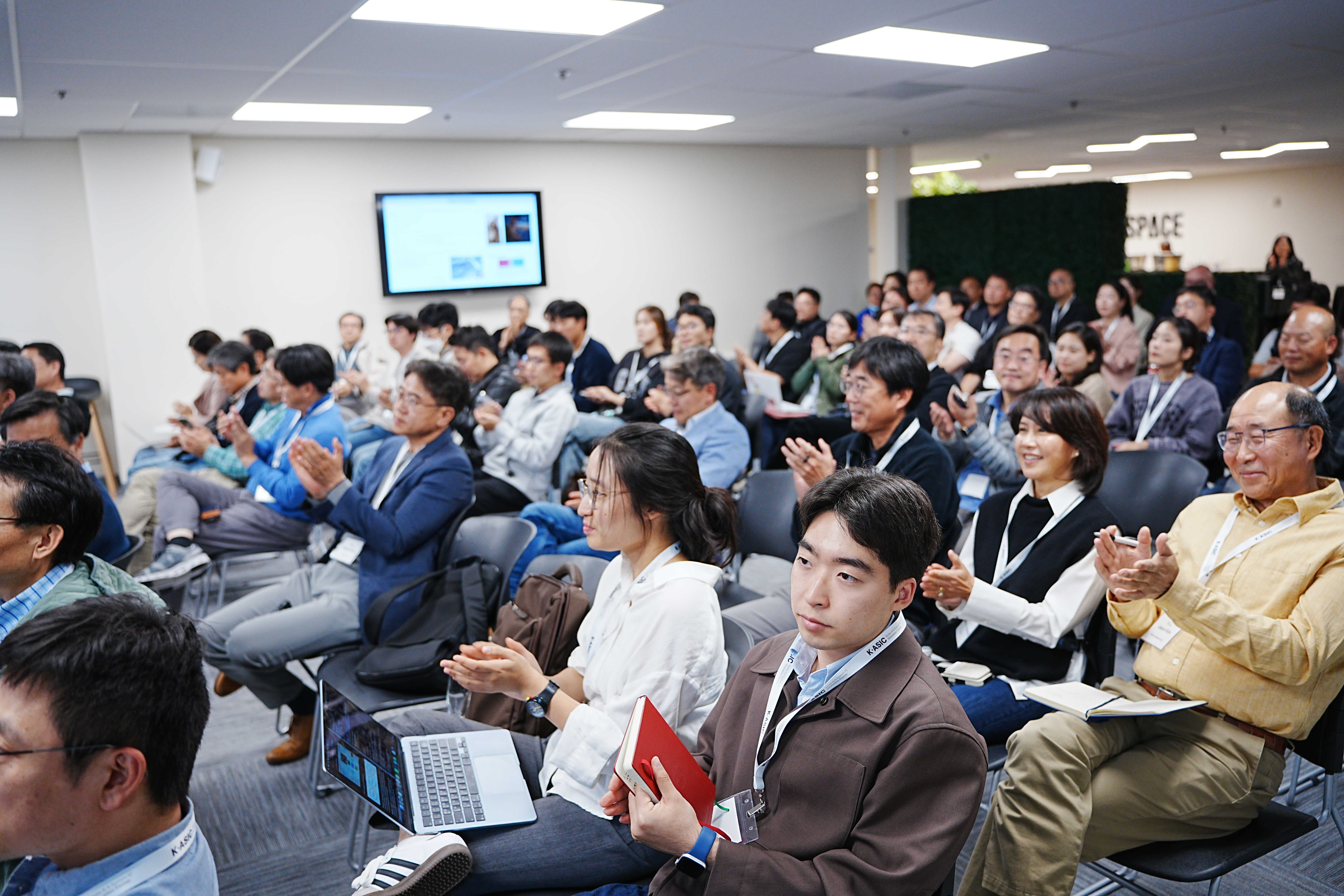
The 13th K-PAI Forum, held on November 12, 2025, at K•ASIC’s Innovation Center in the heart of Silicon Valley, represented far more than another successful technical presentation. The evening marked the first joint seminar between K-PAI and K•ASIC—a strategic alliance that positions both organizations at the forefront of AI semiconductor innovation and Korea-US technological cooperation.
This partnership transcends simple event co-hosting. As we articulated in the opening remarks, this collaboration addresses the most foundational layer of the AI ecosystem. Contemporary AI discourse tends to focus heavily on visible layers—software services, algorithms, and applications—while overlooking the semiconductor infrastructure that makes everything possible. Even within technical domains, hardware constitutes the essential pillar: GPUs (Nvidia’s dominance, partially, only partially though, by Google’s TPUs ★^^☆), HBM (SK hynix’s breakthroughs), specialized AI semiconductors (NPUs, DPUs), custom accelerators from tech giants, and what not!
The strategic partnership between K•ASIC and K-PAI illuminates this foundational layer while connecting Korea’s and America’s semiconductor innovation leadership. This is why we titled this forum “The AI Silicon Race - Korea-US Innovation Leadership.” The event shares the core insight that AI’s future rests on silicon, serving as a venue to explore sustainable development of the global AI ecosystem by consolidating the semiconductor capabilities of both nations.
The Significance of Location
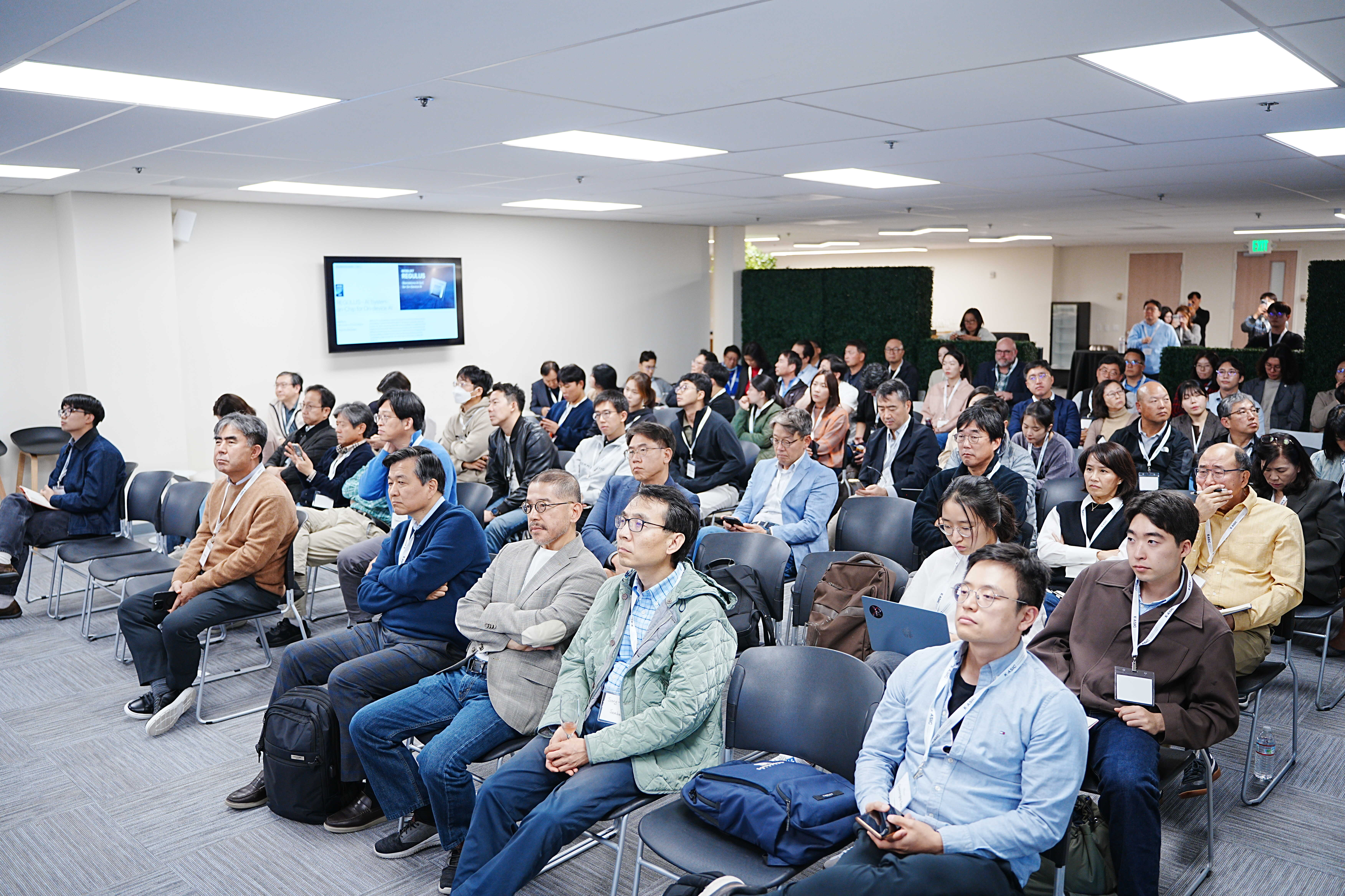
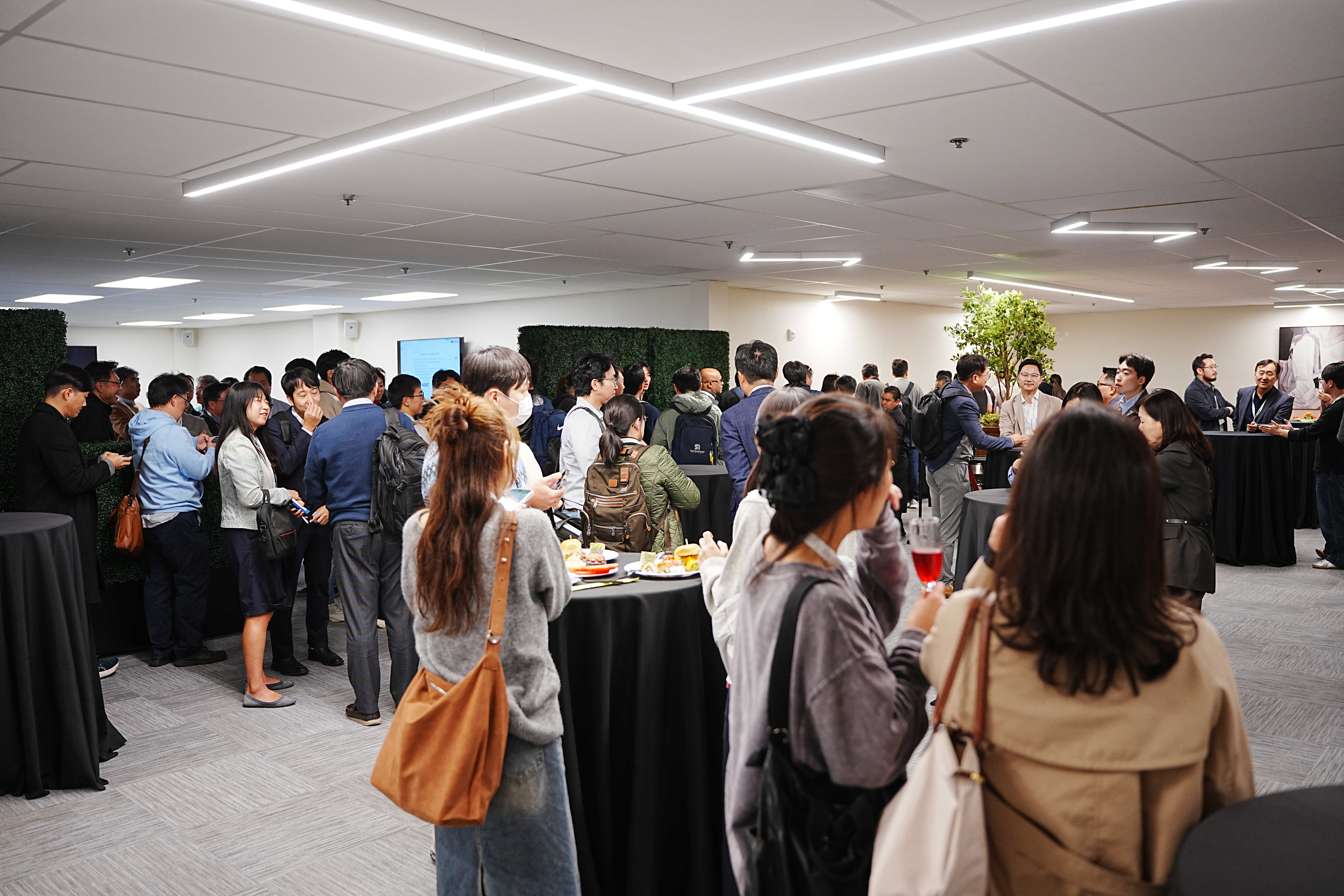
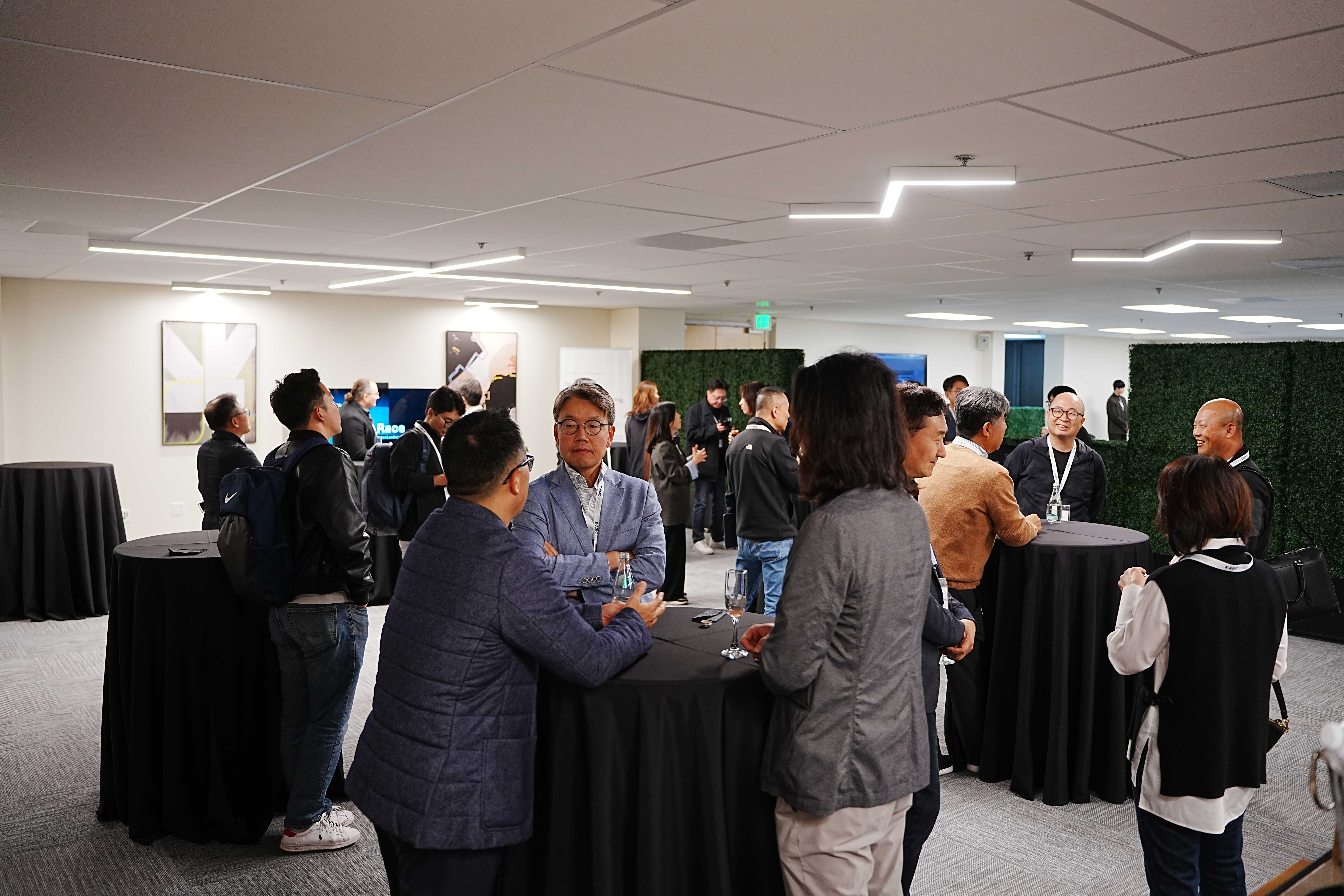
K•ASIC’s state-of-the-art Innovation Center provided more than just a venue—it embodied the partnership’s substance. The facility’s comprehensive event support, including premium signage, professional name badges, and exceptional catering, demonstrated the institutional commitment underpinning this collaboration. More importantly, the center’s role as a bridge between Korean semiconductor excellence and Silicon Valley’s AI ecosystem manifested tangibly through the attendee composition - semiconductor engineers from leading chip companies, AI architects designing next-generation NPUs, hardware entrepreneurs building innovative solutions, and researchers spanning computer architecture, electrical engineering, and systems integration.
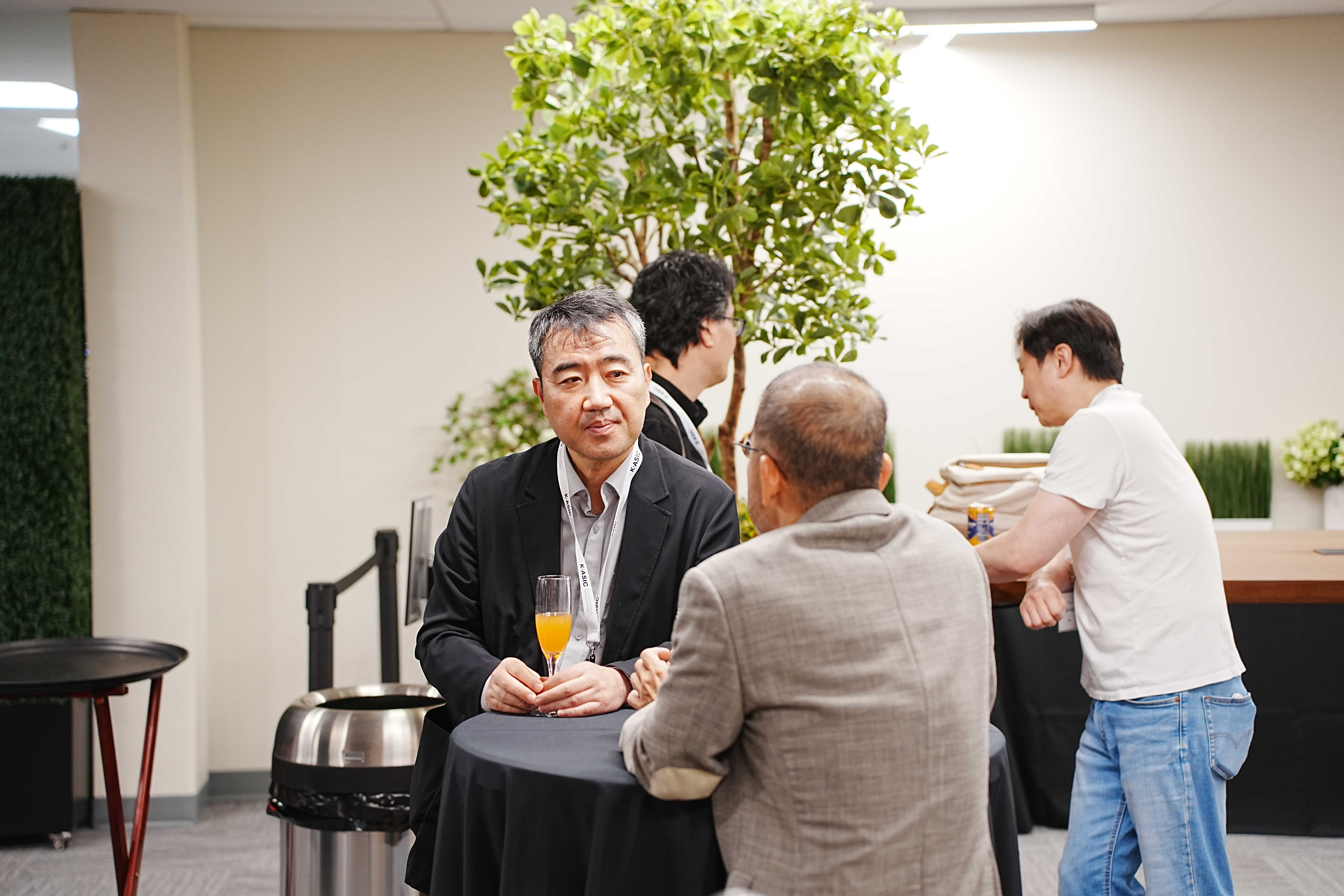
The reception and networking session (5pm - 5:30pm) in K•ASIC’s premium facilities created immediate connections between professionals who are pioneering the next generation of AI silicon. This signature K-PAI networking atmosphere—where genuine technical dialogue emerges naturally rather than through forced mingling—demonstrated how the right venue amplifies community building.
Opening Remarks - Framing Silicon as the Invisible Foundation
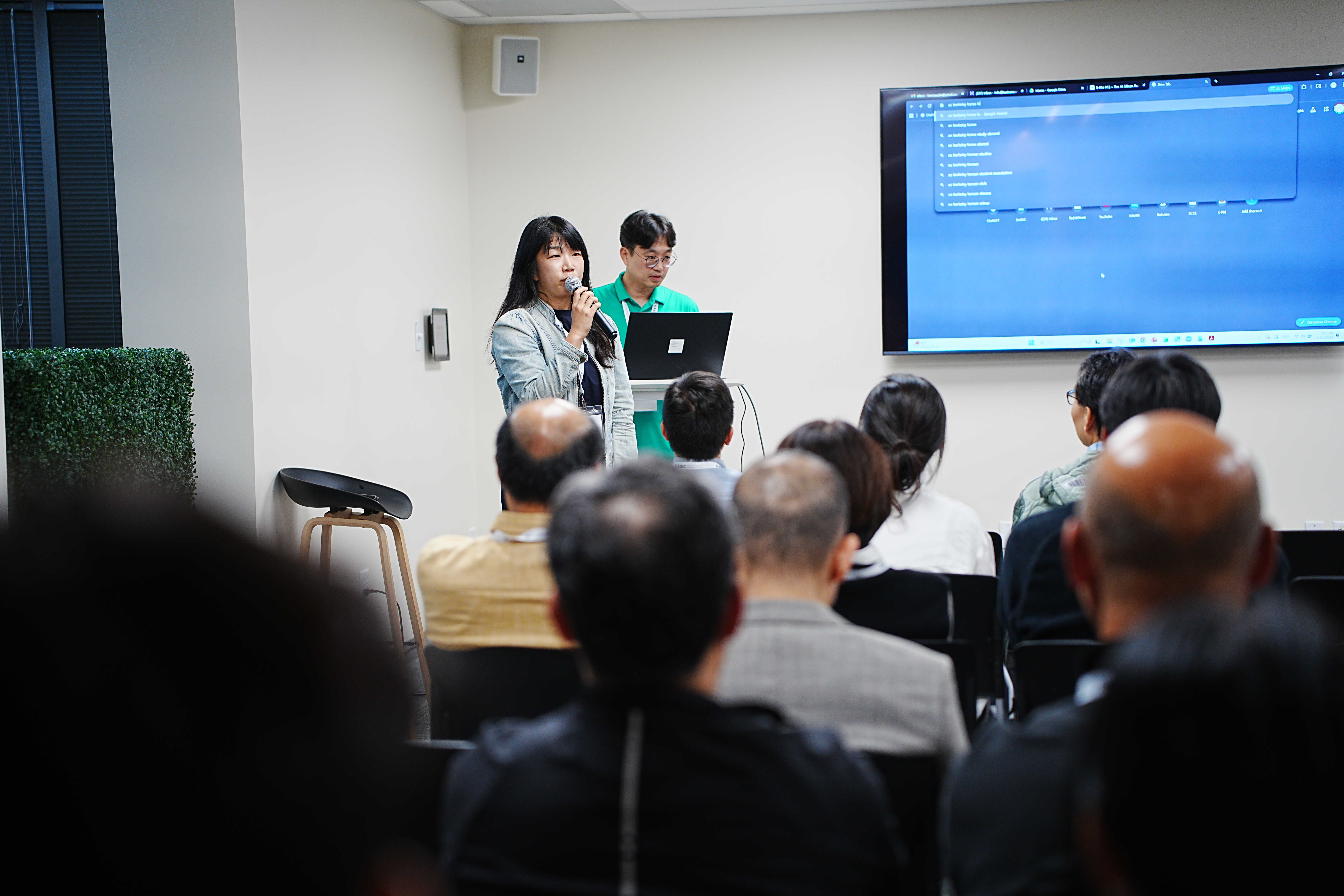
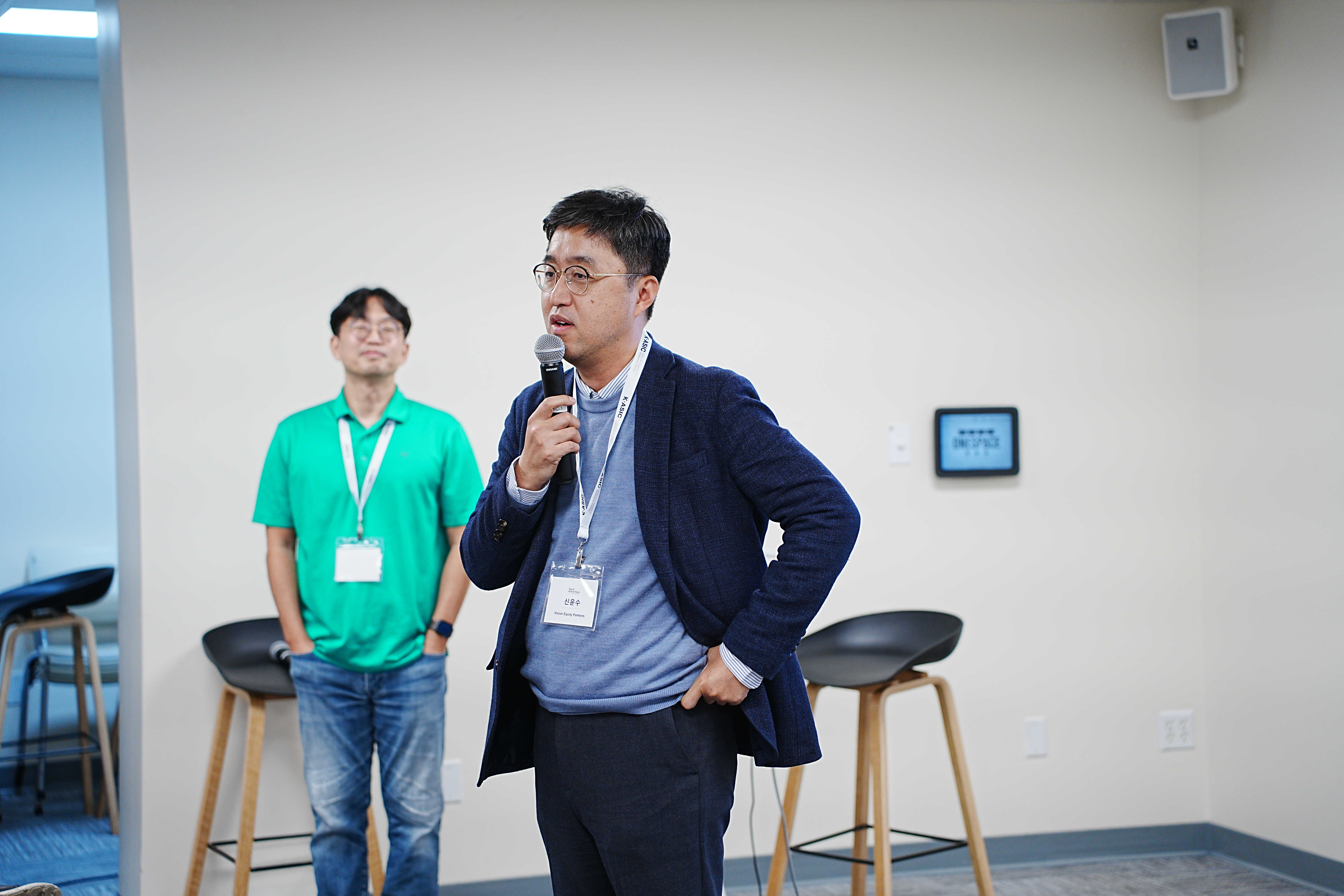
The evening’s opening remarks (5:30pm - 5:40pm) by K-PAI and K•ASIC leadership (Sunghee, Austin, and Kisoo) established the intellectual framework for understanding why this forum represents more than another technical presentation—it illuminates the most foundational yet frequently overlooked layer of the entire AI ecosystem.
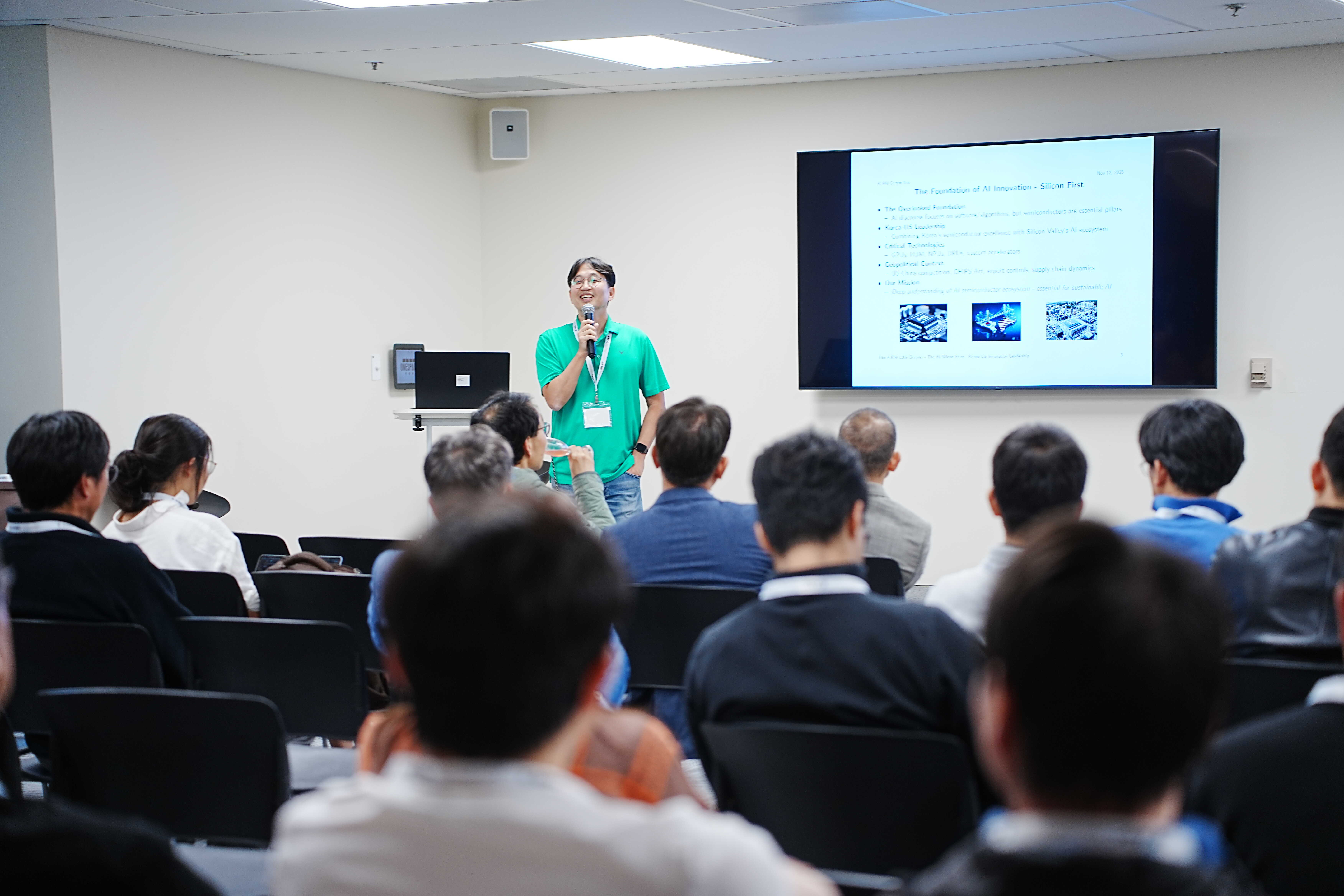
The Overlooked Foundation
As articulated in the opening presentation, contemporary AI discourse exhibits a persistent blind spot. AI discourse focuses on software and algorithms, but semiconductors are the essential pillars upon which everything else rests. Even within technical domains, semiconductor and hardware infrastructure constitute the foundational requirements:
- GPUs - Nvidia’s market dominance reshaping datacenter economics
- HBM - SK hynix’s breakthroughs enabling memory bandwidth scaling
- Specialized AI Semiconductors - NPUs, DPUs, and domain-specific accelerators
- Custom Accelerators - Tech giants’ proprietary silicon (Google TPU, Apple Neural Engine)
This hardware landscape is increasingly shaped by geopolitical dynamics—US-China technology competition, CHIPS Act implementation, export controls tightening, and supply chain restructuring. Understanding and leading sustainable AI development requires deep knowledge of the AI semiconductor ecosystem as absolutely essential rather than optional context.
Korea-US Innovation Leadership - Complementary Strengths
The strategic framing emphasized why we titled this forum “The AI Silicon Race - Korea-US Innovation Leadership.” This partnership transcends simple technical exchange—it recognizes and leverages complementary asymmetric strengths:
- Korea’s Semiconductor Excellence
- world-leading memory technology (Samsung, SK hynix dominance in DRAM and HBM)
- advanced manufacturing capabilities (cutting-edge process nodes)
- high-volume production expertise enabling massive scaling
- decades of accumulated semiconductor manufacturing knowledge
- Silicon Valley’s AI Ecosystem
- algorithm innovation and AI architecture development
- systems integration and software stack sophistication
- entrepreneurial velocity and rapid iteration culture
- close coupling between AI research and commercial deployment
By combining Korea’s semiconductor manufacturing excellence with Silicon Valley’s AI ecosystem innovation, this partnership positions both communities to address the complete stack—from silicon substrates through system architectures to application deployment—in ways neither could achieve independently.
The Mission - Deep Understanding for Sustainable AI
The opening remarks crystallized K-PAI’s evolving mission: deep understanding of AI semiconductor ecosystem is essential for sustainable AI development. This represents a maturation from focusing solely on privacy-preserving techniques or algorithmic innovation toward recognizing that AI’s future depends fundamentally on silicon realities.
Three critical dimensions emerged:
- Technical Sustainability - without continued semiconductor innovation—more efficient architectures, novel memory solutions, advanced packaging—AI scaling faces hard physical limits regardless of algorithmic breakthroughs.
- Economic Sustainability - chip costs, manufacturing capacity, and supply chain resilience determine which AI applications achieve viable unit economics at scale versus remaining research curiosities.
- Geopolitical Sustainability - semiconductor supply chains, manufacturing locations, and technology transfer policies increasingly shape what AI development is even possible for different nations and companies.
The evening’s presentations would explore these dimensions through three complementary lenses: library-based design evolution (Chang), inference economics and architecture (Oh), and edge NPU optimization (Burroughs)—together building comprehensive understanding of how silicon enables and constrains AI futures.
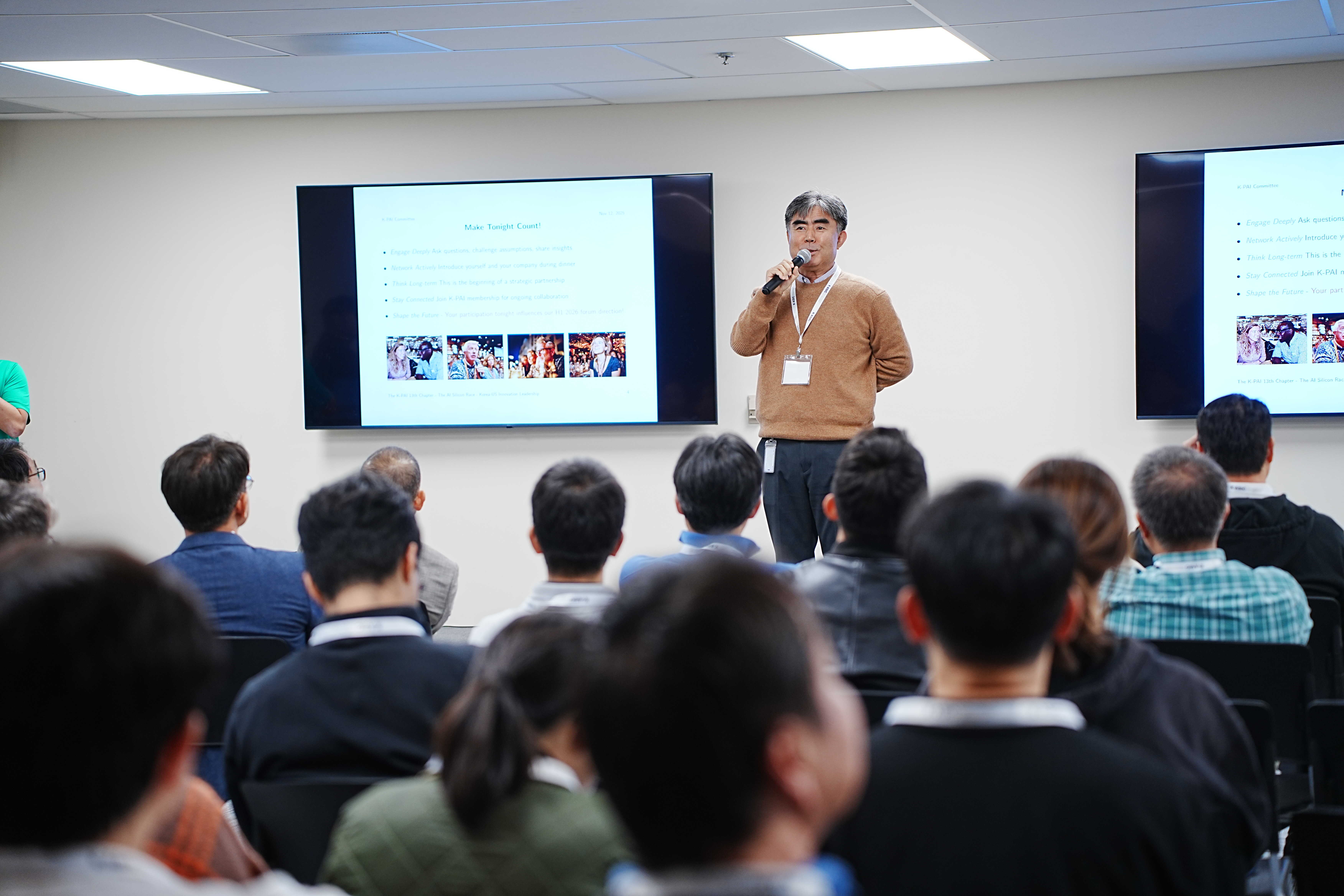
Make Tonight Count - A Call to Active Engagement
The opening concluded with an explicit invitation to active participation rather than passive attendance—five specific imperatives that reflect K-PAI’s community-building philosophy:
- Engage Deeply - Ask questions, challenge assumptions, share insights. The forum’s value multiplies when attendees contribute perspectives rather than merely absorbing content.
- Network Actively - Introduce yourself and your company during dinner. K-PAI’s networking sessions have historically generated transformative partnerships precisely because members view these as professional collaboration opportunities rather than social obligations.
- Think Long-term - This is the beginning of a strategic partnership, not a one-time event. The K-PAI x K•ASIC collaboration creates infrastructure for sustained dialogue spanning years.
- Stay Connected - Join K-PAI membership for ongoing collaboration. The community’s strength derives from continuity—members who engage across multiple forums build cumulative understanding and lasting relationships.
- Shape the Future - Your participation tonight influences our H1 2026 forum direction! The partnership’s flexibility enables responsive topic selection based on community needs and industry evolution.
This participatory ethos distinguishes K-PAI from conventional seminar series. Rather than treating attendees as consumers of expert knowledge, the forums position community members as co-authors and co-creators of an evolving discourse about AI’s responsible development—with semiconductor infrastructure now recognized as equally essential as algorithms, ethics, or applications in that comprehensive understanding.
The Foundation - Library-based Design meets AI Innovation
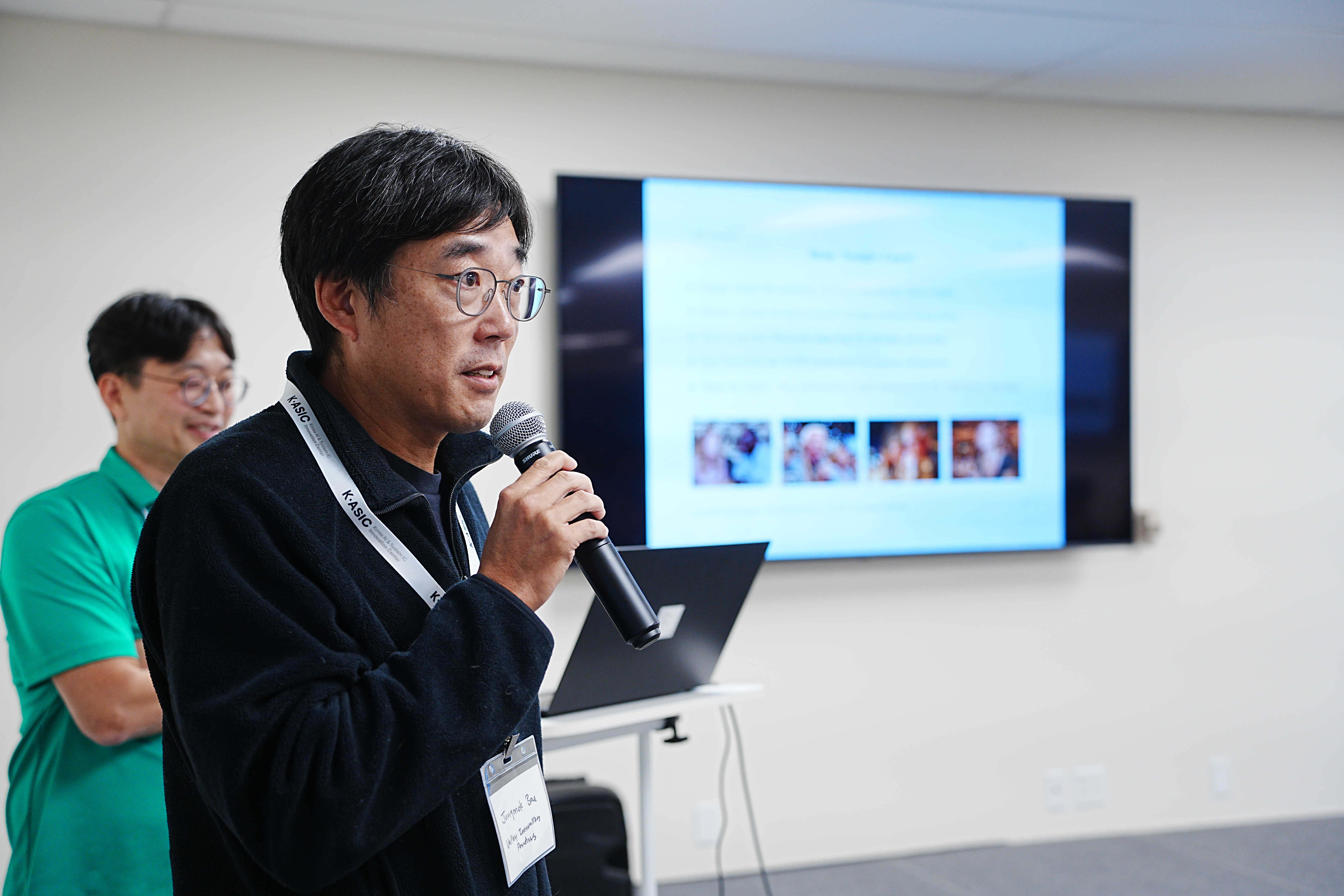
Naehyuck Chang’s Vision - From Standard Cells to Physical AI
Naehyuck Chang’s keynote presentation, “From Semiconductor PPA Optimization to Physical AI - Library-based Design Challenges and New Frontiers,” provided the intellectual foundation for understanding how AI is transforming chip design while simultaneously exploring how chip design principles are transforming AI deployment in physical systems.
Chang brings unparalleled credentials to this discussion—ACM Fellow, IEEE Fellow, former Executive Vice President at Samsung Electronics, and former Technical Program Chair of the prestigious Design Automation Conference (DAC). His career trajectory from Seoul National University through KAIST to Samsung’s highest technical ranks, combined with his extensive experience spanning low-power systems, design automation, battery technology, renewable energy, electric vehicles, and AI algorithms, positions him uniquely to bridge semiconductor design and AI innovation.
The Library-based Design Paradigm
The presentation began by establishing the foundational concept that has driven semiconductor productivity for decades: library-based design. Rather than designing every circuit element from scratch, engineers leverage pre-verified, reusable building blocks—standard cells, IP blocks, analog macros, and layout generators—qualified by foundries or EDA vendors.
Each library element encapsulates domain knowledge, design rules, and performance characterization. Designers focus on system integration and optimization while libraries ensure functional and physical correctness. This process scales from RTL synthesis through layout to verification and sign-off, drastically shortening development cycles.
The key advantages Chang enumerated resonate deeply with anyone who has witnessed semiconductor evolution; Design Time Reduction, Verification Efficiency, Engineer Productivity, Business Alignment, Design Reuse, Technology Migration, and Cross-Domain Application. This last point represents Chang’s crucial insight: the library-based paradigm that revolutionized semiconductor design can now transform how we deploy AI in physical systems.
AI-Driven Optimization - When Intelligence Designs Intelligence
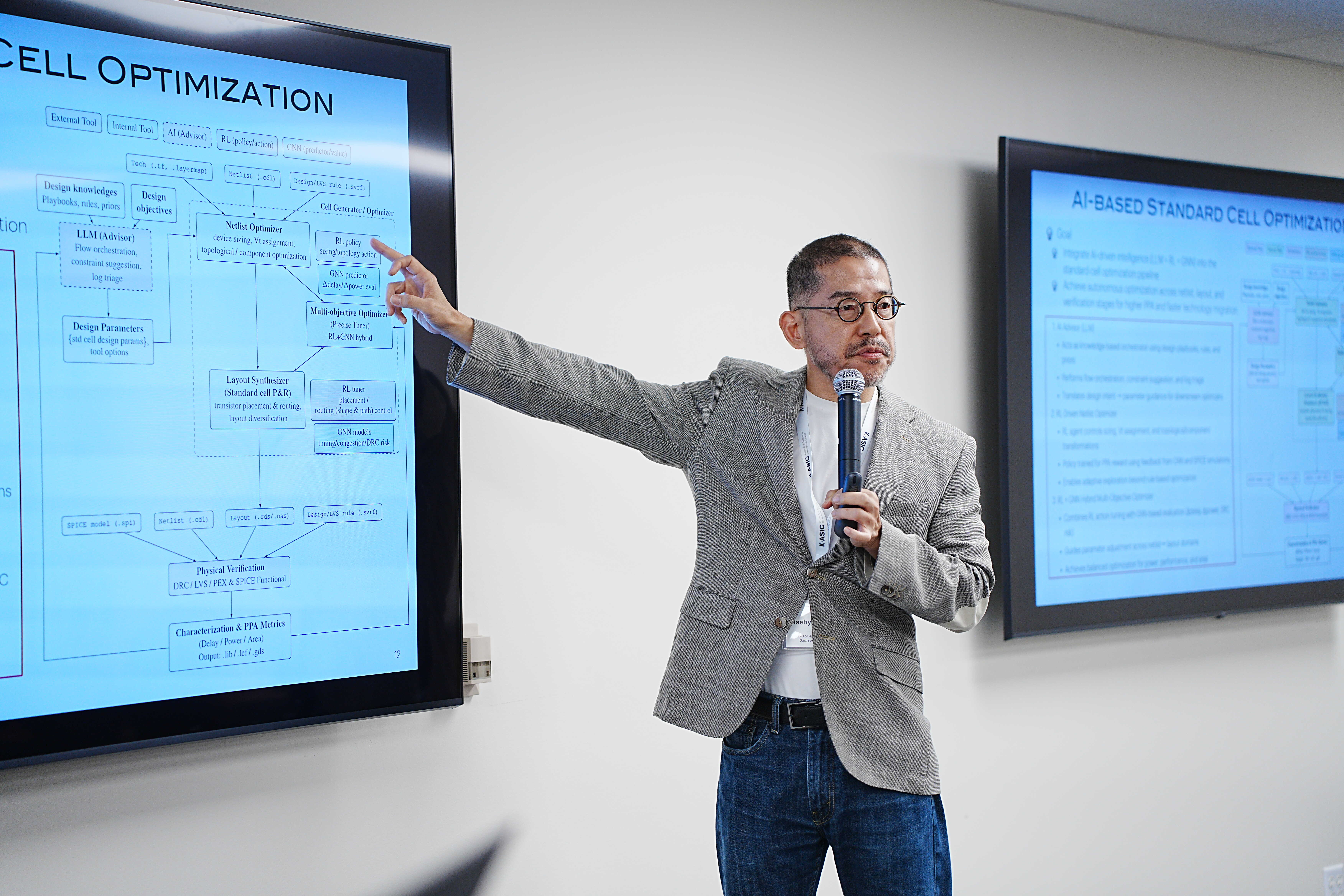
The presentation’s technical core explored how artificial intelligence is optimizing the very silicon that enables AI itself—a recursive relationship with profound implications. Standard cell optimization still has significant room for improvement despite decades of refinement. The conventional layered design process leaves optimization opportunities within standard cell libraries, which play crucial roles in determining power, performance, and area (PPA).
Chang presented Axion’s practical approach using artificial intelligence to improve cell library design and enhance PPA efficiency. The methodology integrates three AI paradigms; AI Advisor (LLM), RL-Driven Netlist Optimizer, GNN-Enhanced Layout Synthesizer, and Verification & Characterization. The integration creates a continuous learning loop where LLM knowledge feeds RL policy, which guides GNN prediction and generates better optimization outcomes. This enables self-improving cell generation, rapid PPA closure, and scalable technology migration without requiring expert-level system knowledge.
The implications extend far beyond individual cell optimization. As I reflected in recent writings on AI’s energy challenges, every efficiency gain at the silicon level multiplies across billions of operations, potentially addressing the existential energy constraints facing AI scaling. Chang’s work demonstrates that AI can help solve its own infrastructure challenges through recursive self-improvement at the foundational hardware layer.
Physical AI - The Convergence of Control, Systems, and Intelligence
The second half of Chang’s presentation introduced a future-oriented vision: Physical AI, which combines control intelligence with physical systems. This concept extends the library-based design philosophy from semiconductors to embodied intelligent systems—robotics, manufacturing, industrial design, autonomous vehicles, and smart infrastructure.
Chang articulated the Physical AI vision compellingly: bridging control, systems, and AI domains through integrated policy development, encapsulating domain knowledge into pretrained reusable libraries for scalable deployment, and enabling PPA enhancement via end-to-end learning across design, control, and physical systems.
The Pretrained Physical AI Libraries concept mirrors semiconductor library evolution. Just as Axion Cell library optimization originates from control-system expertise and Design Automation of Things (DAoT) principles, Physical AI libraries encapsulate specialized knowledge in specific domains: vision and perception algorithms, robot motion control theory, classical control technologies, position and attitude control methods.
Remarks - The Chemistry between Electrical Engineering and Computer Science
Chang’s closing remarks offered a philosophical reflection that resonated powerfully with K-PAI’s interdisciplinary ethos. He articulated his lifetime goal: “To build and sustain a collaborative culture that achieves genuine, chemistry-level integration between Electrical Engineering and Computer Science.”
The question he posed—”Why chemistry mixing? Is CS and EE interface a border city or a PN junction?”—cuts to the heart of how we structure knowledge domains and professional communities. A border city implies separate territories with occasional crossing points. A PN junction suggests fundamental integration where the interface itself creates entirely new properties—the depletion region where electrons and holes recombine to form something neither domain alone possesses.
This vision aligns perfectly with K-PAI’s founding principles—that the most transformative innovations emerge at disciplinary boundaries, where distinct bodies of knowledge create new synthesis through genuine integration rather than superficial collaboration.
NPU Architecture Evolution
Richard Burroughs, Vice President at Mobilint, Inc., presented “AI Starts Here - 온디바이스 AI 시대, 경량화된 NPU 아키텍처의 진화” (Lightweight NPU Architecture Evolution in the On-Device AI Era).
Burroughs’ presentation explored how Neural Processing Unit (NPU) architectures are evolving to meet on-device AI demands—examining architectural innovations enabling efficient inference from quantization techniques and model compression to novel dataflow architectures and memory hierarchies optimized for neural network workloads.
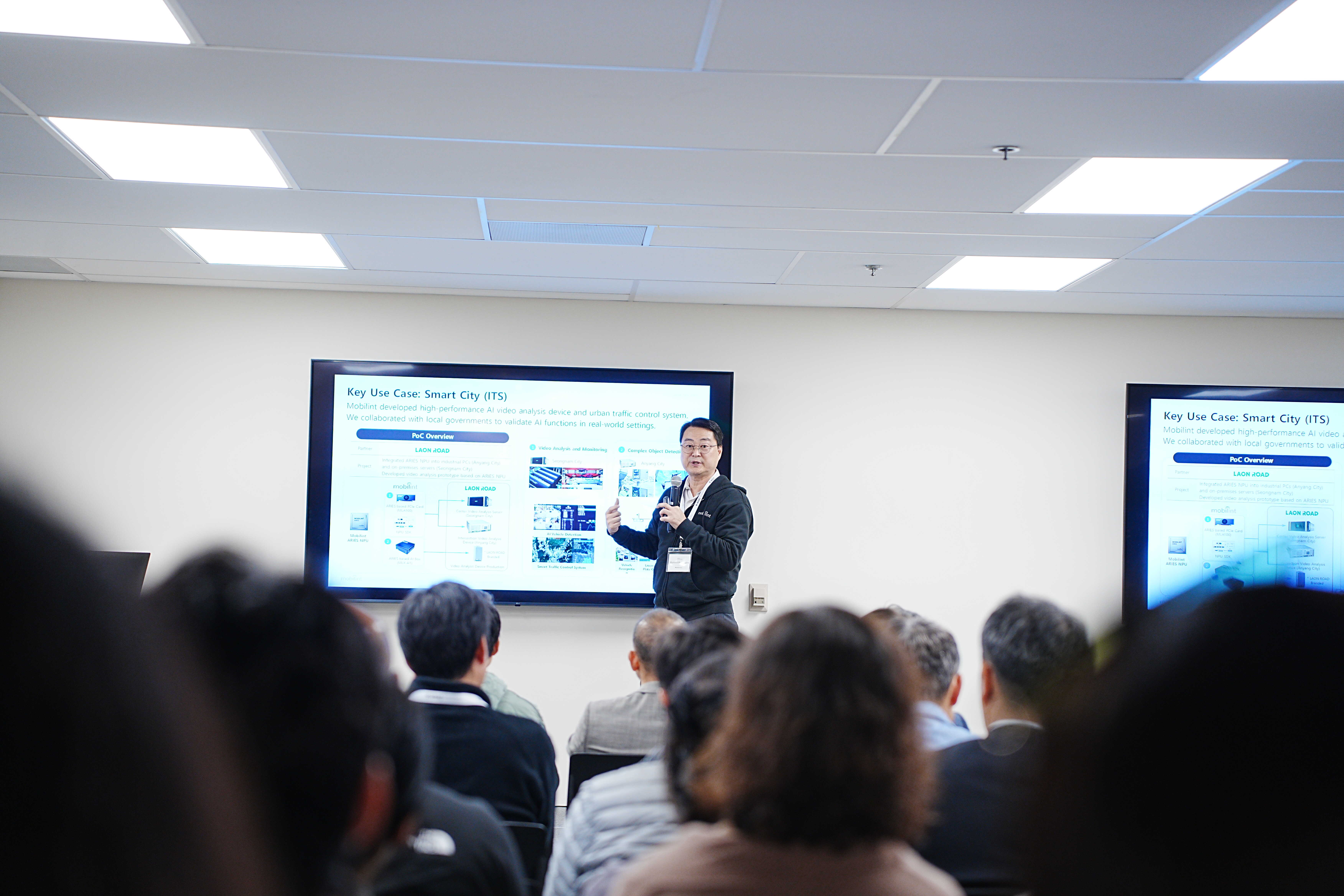
The presentation demonstrated how NPU evolution enables sophisticated AI capabilities in smartphones, IoT devices, and embedded systems while maintaining strict power budgets and thermal constraints—providing insights into design tradeoffs between computational throughput, power efficiency, and silicon area.
This perspective represented an important dimension of the AI silicon ecosystem - while datacenter chips pursue maximum performance within generous power envelopes, edge NPUs must deliver acceptable intelligence within milliwatt budgets and consumer product thermal constraints. The architectural innovations enabling this—specialized datapaths, aggressive quantization, model-architecture co-design—represent equally sophisticated engineering as datacenter accelerators but with fundamentally different optimization objectives.
Future K-PAI forums might explore this edge AI dimension more deeply, potentially examining how architectural choices at the edge (NPUs in smartphones, automotive processors, IoT chips) differ from datacenter acceleration and how these distinct optimization regimes might inform each other.
The Economics - Bridging Performance and Affordability
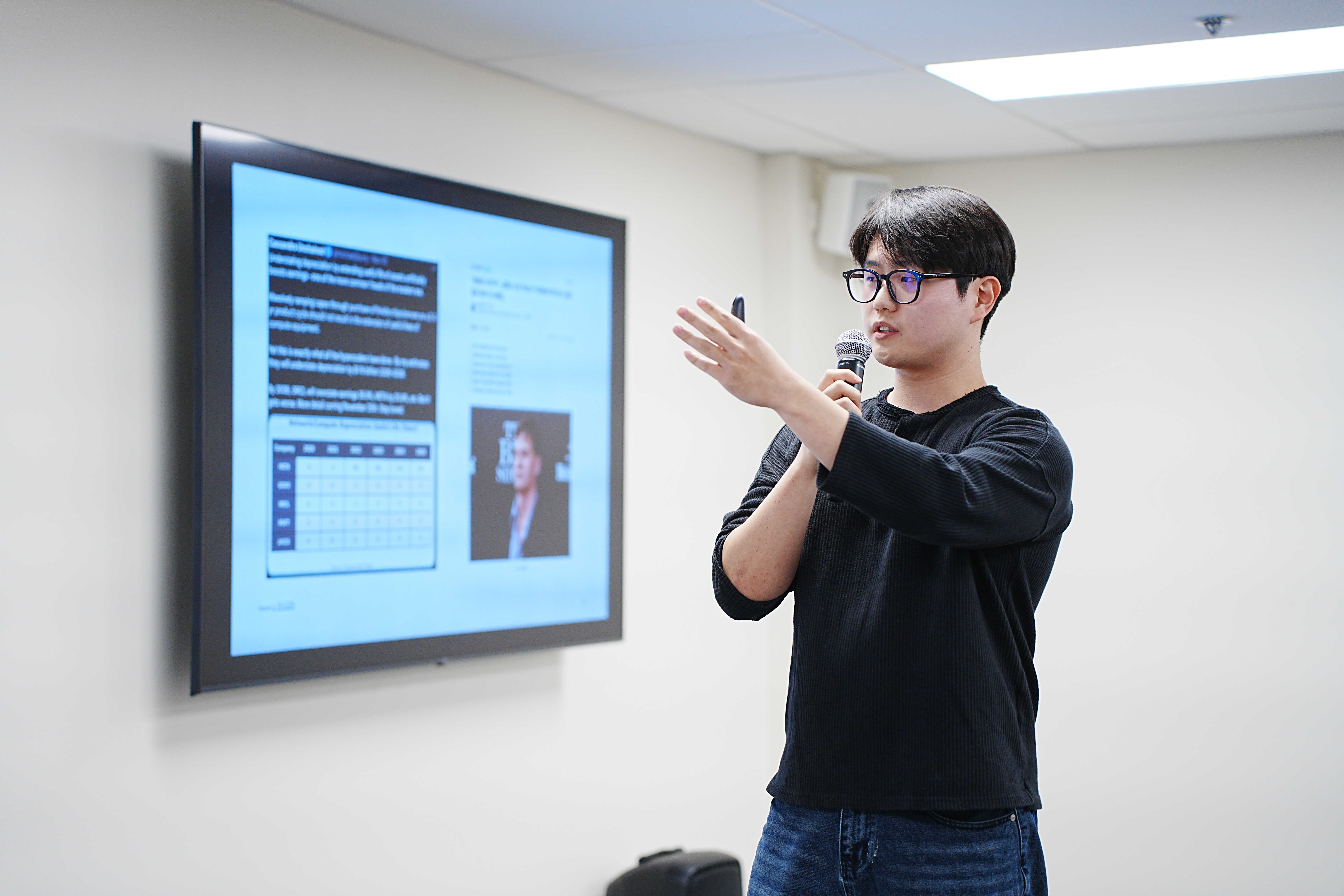
Juntaek Oh’s Market Reality - HyperAccel’s Pragmatic Approach
Juntaek Oh, Compiler Engineer at HyperAccel, brought a complementary perspective grounded in stark market realities and entrepreneurial pragmatism. His presentation, “Bridging Performance and Affordability in AI Silicon,” addressed the critical tension between cutting-edge computational capabilities and cost-effective implementations.
The Trillion-Dollar Context
Oh opened with vivid illustrations of the massive capital flows reshaping AI infrastructure. The images of tech CEOs meeting casually—the famous photo that circulated in Korean media showing industry titans sharing drinks and discussing billions in GPU purchases—established the scale of investment driving AI semiconductor demand.
The market data painted an urgent picture:
- AMD CEO Lisa Su projects the AI data center market reaching $1 trillion by 2030
- Meta plans $600 billion US spend as AI data centers expand
- Google Cloud launches Ironwood TPUs and new Axion VMs for AI inference
- Nvidia announces 26 major AI chip customers with $65 billion of committed orders
Yet beneath this apparent gold rush lies troubling complexity. The Cassandra Unchained analysis Oh presented revealed uncomfortable truths about depreciation accounting: hyperscalers may understate depreciation by $176 billion from 2026-2028 through artificially extended useful lives of AI equipment. By 2028, Oracle could overstate earnings by 26.9%, Meta by 20.8%—accounting practices that mask the true economics of AI infrastructure deployment.
The energy constraints add another dimension of urgency. MIT News analysis estimates that by 2030, all generative AI queries will consume 347 TWh—equivalent to 44 nuclear reactors’ annual output. Even 100MW data center capacity may remain unused for years due to power shortage, according to supply chain analyses. The infrastructure cannot keep pace with computational demand.
HyperAccel’s LPU Vision - Specialized Excellence
HyperAccel’s approach crystallized around a fundamental insight: training and inference represent fundamentally different computational patterns requiring different silicon architectures.
- Training (Model Making) - Large batch sizes enabling high parallelism, Compute-intensive operations dominating workload, and Throughput-oriented optimization.
- Inference (Service Deployment) - Small batch sizes (often individual requests), Memory-intensive patterns (model parameter access), and Latency-oriented requirements for user experience.
GPUs excel at training’s parallel compute patterns but prove inefficient for inference’s sequential, memory-bound characteristics. HyperAccel’s LPU (LLM Processing Unit) architecture specifically targets the Transformer’s large models and sequential processing demands.
The Technical Differentiation: LPDDR vs HBM
Oh’s presentation detailed HyperAccel’s key innovation: replacing expensive HBM (High Bandwidth Memory) with standard LPDDR memory. The advantages compound:
- Cost Efficiency - LPDDR costs approximately ½ the price of HBM, No expensive HBM advanced packaging required, and Comparatively lower IP licensing costs.
- Supply Availability - LPDDR is widely available vs. HBM supply constraints and 2x the maximum capacity of current HBM implementations.
- Power Efficiency - 60% less power consumption than HBM and Critical for total cost of ownership in datacenter deployments.
- Architectural Optimization - Streamlined memory access patterns maximizing bandwidth utilization, Specialized compute engines for end-to-end LLM operations, and Matrix and vector execution engines purpose-built for Transformer architecture.
The full-stack HyperDex software platform ensures developers experience seamless transition from GPU environments—using same OpenAI API requests, running vLLM OpenAI-compatible server, accessing models from HuggingFace Hub. This software compatibility removes adoption friction while hardware delivers superior economics.
Performance Claims and Market Positioning
HyperAccel’s performance assertions are striking: 2X higher throughput, 20X better cost efficiency, and 5X better energy efficiency compared to Nvidia H100 (for Llama 3.1 70B workloads). If validated at scale, these metrics would fundamentally reshape datacenter AI economics.
The datacenter cost reduction analysis Oh presented demonstrated how chip-level improvements cascade through total infrastructure costs:
- Chip cost reduction (90% savings: $3,850 vs $40,000 per chip)
- Energy savings (60% reduction in power consumption)
- Combined impact: 17.6% reduction in total datacenter operating costs
For hyperscalers deploying thousands of chips, even incremental percentage improvements in efficiency translate to hundreds of millions in annual savings.
Product Roadmap: From FPGA to ASIC
HyperAccel’s pragmatic roadmap demonstrates mature understanding of semiconductor commercialization - Orion LPU FPGA Server (4Q 2023), Silicon Prototype (4Q 2024), LPU ASIC-DC Chip (1Q 2026), and LPU ASIC-Edge Chip (4Q 2026).
This staged approach—FPGA prototype enabling rapid iteration, followed by datacenter ASIC, then edge deployment—mirrors successful semiconductor startup patterns while demonstrating capital-efficient development.
The Affordability Imperative
Oh’s presentation title—”Bridging Performance and Affordability”—captured an essential tension in AI silicon development. The industry has demonstrated it can build ultra-high-performance chips (H100, TPU v5) but at price points that limit deployment breadth. HyperAccel’s thesis is that the inference market demands different tradeoffs: sufficient performance for quality user experience, but at costs enabling widespread deployment rather than concentration in hyperscaler datacenters alone.
This democratization narrative—making AI infrastructure accessible beyond the biggest tech companies—aligns with broader industry trends toward edge AI, on-device processing, and distributed intelligence. If specialized inference chips can deliver acceptable performance at fractional costs, entirely new categories of AI applications become economically viable.
Thematic Synthesis - The Layered AI Stack
From Applications to Silicon - Cumulative Understanding
The progression from October’s marketing AI focus through November’s semiconductor exploration demonstrates K-PAI’s evolving sophistication in creating narrative arcs across forums rather than treating each event in isolation.
The 12th forum examined how AI transforms advertising through intelligent optimization—video analysis, budget allocation, programmatic systems. These capabilities rest on assumptions about available computational resources. Park’s ADOASIS platform analyzes thousands of videos using computer vision and NLP models. Ko’s DSP architectures employ deep neural networks for retrieval and ranking. Both applications demand massive parallelizable computation that only modern AI accelerators enable.
The 13th forum explored the silicon layer making these applications possible:
- How are AI chips designed? (Chang’s library-based optimization, AI-driven standard cells)
- What architectural choices enable performance and efficiency? (HyperAccel’s LPU, memory hierarchy optimization)
- Where do supply chain vulnerabilities threaten AI scaling? (HBM supply constraints, energy limitations)
- How do Korea and United States collaborate to maintain semiconductor leadership? (K•ASIC partnership, complementary strengths)
This layered approach—applications in October, enabling hardware in November—creates cumulative understanding of the complete AI stack. Attendees gain appreciation not just for what AI can do but for what makes it possible (specialized silicon, advanced memory, efficient manufacturing).
The Korea-US Semiconductor Alliance
The forum’s subtitle—”Korea-US Innovation Leadership”—reflects genuine complementary strengths rather than political rhetoric:
Korea’s Manufacturing Excellence: Samsung and SK hynix leadership in memory technologies (HBM, LPDDR), advanced packaging (2.5D/3D integration), and high-volume manufacturing provides production capacity that AI scaling demands. Korean foundries’ process technology expertise (4nm, 3nm nodes) enables cutting-edge chip fabrication.
US Design Innovation: American companies’ dominance in chip architecture design (GPU, TPU, custom accelerators), EDA tools (Synopsys, Cadence), and systems integration creates intellectual foundation for next-generation AI hardware. Silicon Valley’s concentration of AI expertise enables tight coupling between algorithm development and hardware optimization.
Shared Strategic Interests: Both nations face similar challenges from China’s semiconductor ambitions and share interests in maintaining technological leadership, supply chain security, and access to critical manufacturing capabilities. The geopolitical dimension—export controls, CHIPS Act, technology transfer restrictions—makes Korea-US cooperation strategically essential beyond purely commercial considerations.
The K-PAI x K•ASIC partnership embodies this alliance at the community level, creating venues where Korean semiconductor engineers and Silicon Valley AI architects exchange insights, identify collaboration opportunities, and build relationships that could mature into commercial partnerships or joint development programs.
Physical AI - The Convergence Horizon
Chang’s Physical AI vision represents perhaps the forum’s most forward-looking theme—suggesting how the boundaries between digital intelligence (software, algorithms) and physical systems (robotics, manufacturing, infrastructure) will increasingly blur.
The library-based design paradigm’s extension from semiconductors to physical systems mirrors historical patterns where successful abstractions in one domain eventually generalize to others. Just as object-oriented programming principles migrated from software to hardware description languages, library-based design concepts are now migrating from chips to robots.
The implications extend far beyond individual applications:
- Standardization and Interoperability - Pretrained Physical AI libraries could enable standardized interfaces between perception, control, and actuation subsystems—reducing integration complexity similar to how standard cells simplified chip design.
- Skill Democratization - Just as semiconductor libraries enabled designers without deep physics knowledge to create functional chips, Physical AI libraries might enable robotics applications without requiring control theory expertise or deep systems understanding.
- Rapid Iteration - The ability to compose physical systems from pretrained, validated components could accelerate deployment cycles from years to months—matching the pace of software development rather than traditional hardware timelines.
- Domain Knowledge Preservation - Encapsulating expertise from controls engineers, systems designers, and domain specialists into reusable libraries preserves institutional knowledge beyond individual careers while making it accessible to new generations.
The convergence of AI optimization (learning optimal policies), physical constraints (material properties, dynamics), and systems integration (coordinating multiple subsystems) represents exactly the kind of cross-disciplinary synthesis that K-PAI’s forums are designed to explore and accelerate.
Community Dimensions - More Than Technical Exchange
The Networking Imperative
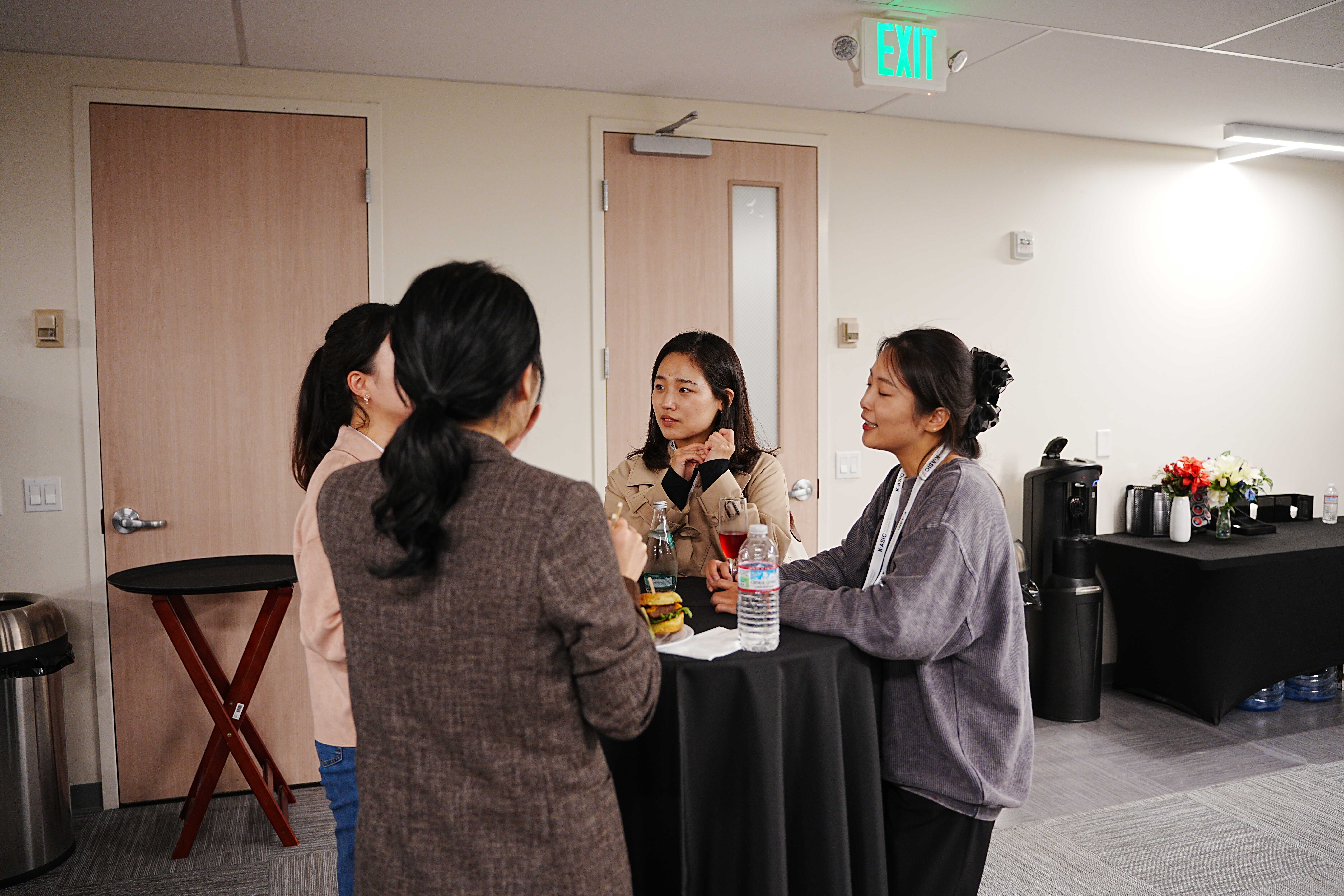
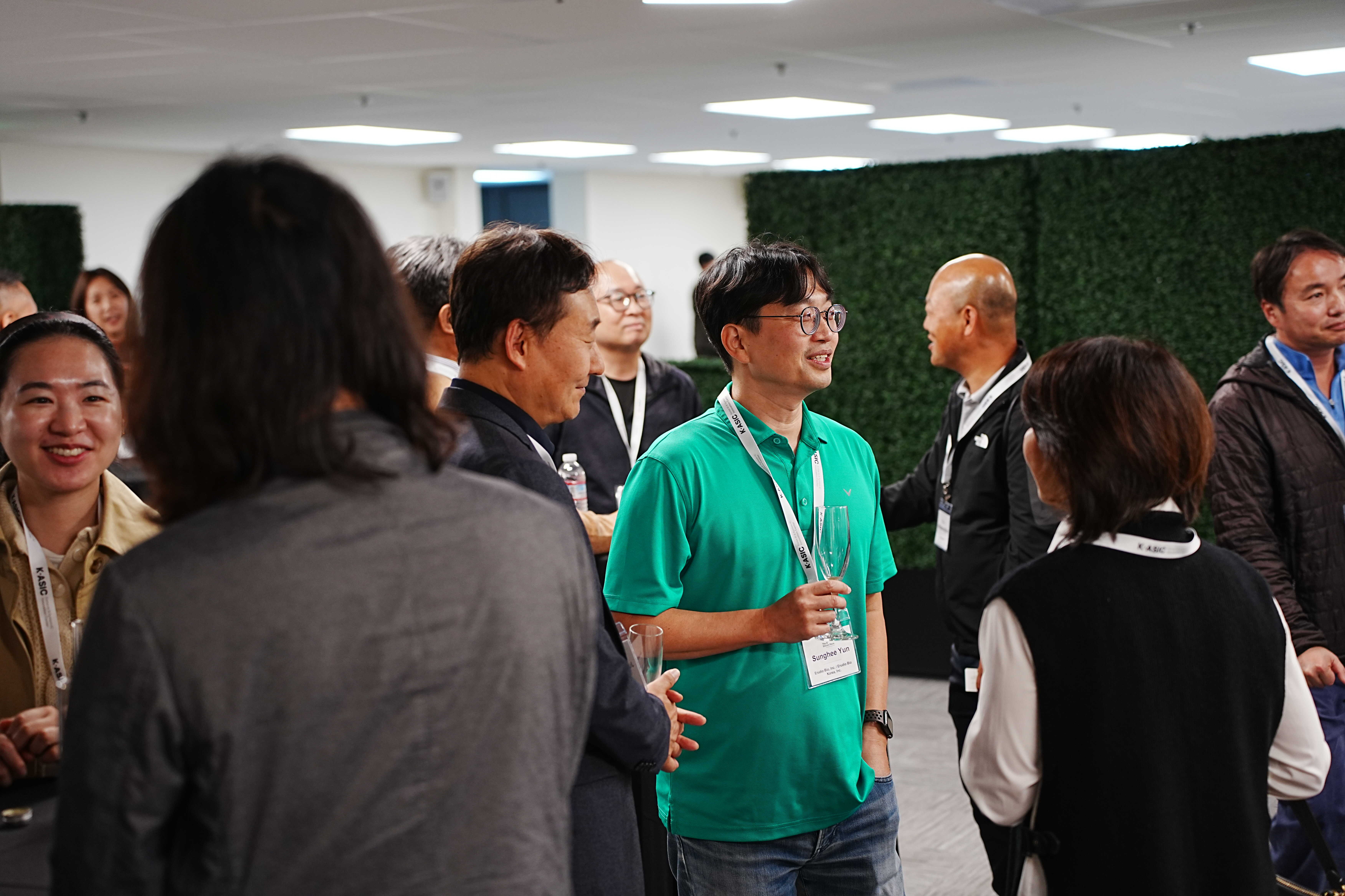
The extended networking dinner and Q&A session (7pm - 8pm) provided what many attendees described as the forum’s highest-value component. K-PAI members are encouraged to introduce themselves and their companies, creating opportunities for meaningful business connections and potential collaborations in the rapidly evolving AI hardware space.
Previous forums have seen transformative partnerships emerge during these dynamic discussions, where hardware engineers, AI researchers, chip designers, and entrepreneurs bridge technical challenges with innovative solutions in real-time conversations. The semiconductor focus attracted a particularly rich attendee mix—architects from leading chip companies, startup founders developing novel accelerators, investors evaluating AI hardware opportunities, and researchers exploring new computational paradigms.
The conversations that continued well past the scheduled conclusion revealed genuine enthusiasm about both the specific technical insights shared and the broader implications for participants’ work. Semiconductor engineers discovered how AI optimization techniques could improve their chip design workflows. AI researchers gained appreciation for the hardware constraints shaping what’s architecturally possible. Entrepreneurs identified specific technical bottlenecks where novel solutions might create differentiated value.

The Partnership Model in Action
The K-PAI x K•ASIC collaboration demonstrated institutional partnership benefits tangibly:
- Venue Access - K•ASIC’s state-of-the-art Innovation Center provided professional facilities that would be prohibitively expensive for an independent organization to secure, while embodying the semiconductor focus thematically.
- Network Leverage - K•ASIC’s connections throughout Korean semiconductor industry facilitated speaker recruitment and attendee engagement that would be difficult to achieve through cold outreach alone.
- Content Expertise - K•ASIC’s technical leadership provided guidance on forum themes, speaker selection, and content depth—ensuring discussions matched industry needs rather than academic abstractions.
- Operational Support - Comprehensive event logistics—signage, name badges, catering, technical setup—enabled K-PAI organizers to focus on content quality and community building rather than administrative details.
This partnership model creates sustainable infrastructure for ongoing dialogue rather than episodic events requiring repeated resource mobilization. The commitment to minimum twice-yearly co-hosted forums establishes predictable cadence while the perpetual nature enables long-term planning and cumulative community development.
Looking Forward - The H1 2026 Second Forum
The announcement of a second K-PAI x K•ASIC joint forum planned for H1 2026 with expanded scope and impact creates immediate anticipation. Potential themes building on the 13th forum’s foundation might include:
- Advanced Packaging and Chiplet Architectures - Exploring how 2.5D/3D integration, chiplet-based designs, and heterogeneous integration enable next-generation AI systems while managing manufacturing complexity and cost.
- Memory Innovation Beyond HBM - Examining emerging memory technologies (processing-in-memory, near-memory compute, novel memory hierarchies) that could address the memory bandwidth bottleneck limiting AI accelerator performance.
- AI for Chip Design - Deeper exploration of how machine learning is automating and optimizing semiconductor design flows—from architecture exploration through physical design to verification and test.
- Edge AI and Embedded Intelligence - Comprehensive examination of architectural approaches for on-device AI, including NPU evolution, quantization techniques, model-architecture co-design, and power management strategies.
- Geopolitical Dimensions of AI Silicon - Strategic analysis of how semiconductor supply chains, export controls, manufacturing capacity, and international partnerships shape AI development trajectories and competitive dynamics.
The flexibility to define topics based on industry evolution and community feedback demonstrates the partnership’s responsiveness while the institutional commitment ensures continuity regardless of short-term market fluctuations.
Conclusion - Silicon First
The 13th K-PAI Forum successfully illuminated AI’s most essential yet frequently overlooked layer—the semiconductor infrastructure enabling all innovation above. Through Chang’s exploration of library-based design evolution and AI-driven optimization, through Burroughs and Oh’s pragmatic examination of inference economics and architectural tradeoffs, the evening built compelling argument that understanding AI futures requires understanding silicon realities.
The historic K-PAI x K•ASIC partnership launch provided more than symbolic significance—it created institutional infrastructure for sustained dialogue between Korea’s semiconductor manufacturing leadership and Silicon Valley’s AI algorithm innovation. This partnership positions K-PAI at the nexus of two critical technology domains while advancing the organization’s evolution from technical education toward strategic discourse.
Most fundamentally, the forum reinforced that AI development cannot be divorced from its silicon substrate. Algorithmic innovation, application creativity, and business model ingenuity all ultimately constrain against what’s physically implementable in semiconductor technology at economically viable cost points within acceptable power budgets.
The companies and communities that will succeed in the AI era are those developing integrated strategies addressing algorithms, applications, and architectures simultaneously—recognizing that breakthrough AI capabilities emerge from co-optimization across these traditionally separate domains rather than from excellence in any single dimension.
The K-PAI community is building exactly this kind of holistic understanding through cumulative forum experiences—October’s marketing applications, September’s energy infrastructure, August’s legal frameworks, and now November’s semiconductor foundations. Each perspective enriches understanding of others, creating systems-level comprehension rather than narrow technical specialization.
As we look toward the H1 2026 second K-PAI x K•ASIC joint forum, the foundation established by this inaugural collaboration creates exciting possibilities for deeper exploration—advanced packaging, memory innovation, AI-for-chip-design, edge intelligence, or geopolitical semiconductor dynamics. The partnership’s flexibility enables responsive topic selection matching industry evolution while institutional commitment ensures continuity.
The energy pervading the networking session—semiconductor engineers, AI architects, hardware entrepreneurs, and researchers engaged in animated technical discussions extending well beyond scheduled conclusion—reflected genuine community enthusiasm about both the specific insights shared and the broader vision of Korea-US semiconductor cooperation enabling sustainable AI innovation.
The 13th K-PAI Forum proved that innovation thrives at intersections: between disciplines (EE and CS), between nations (Korea and US), between domains (digital and physical), and between organizations (K-PAI and K•ASIC). By illuminating the foundational silicon layer, the evening demonstrated that AI’s future will be built not only on elegant algorithms but on sophisticated semiconductor engineering—requiring deep cross-disciplinary understanding and sustained international collaboration to realize technology’s full potential while serving humanity’s broader interests.